
 Outline of the Center of Excellence Program Outline of the Center of Excellence Program
Atsushi Iwata
COE leader,
Principle of the COE
For more than twenty years, we have focused our attention on mainstream progress in silicon integrated circuit technology along with the worldÕs top-level research and developments in VLSI technology, which are seen to be the keys to the realization of an advanced information society. Building upon this solid foundation, the objectives of the COE are the development of fundamental technologies and new academic fields for a new integration system based on the design principles of both physical and information processing theory. We also plan to establish a novel, highly innovative system with advanced recognition/learning functions utilizing the integration of silicon nano-devices, circuits, and architectures.
From an academic perspective, we aim to construct new fields of research by integrating circuit design and device processing technologies, currently disparate disciplines, using device modeling techniques as cross-linkers. It is important to educate many specialists with the critical abilities necessary to both research and develop a wide range of electronics-based academic fields. Therefore, we aim to foster and support promising individuals with the ability to approach technological challenges with a deep understanding and practical capability to facilitate the promotion of advanced independent research.
Core members and major achievements of the COE group (Fig.1)
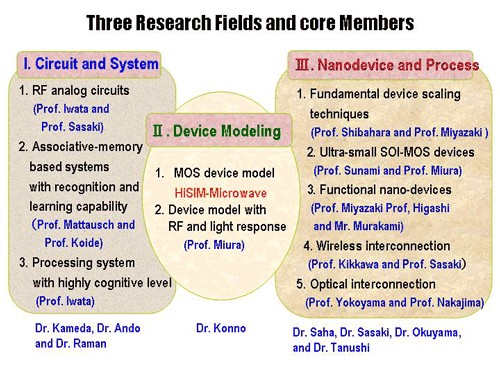
Over the past 30 years, our group has achieved top-level results in the following three fields in the area of research and education of silicon integrated circuits.
First, in the field of ÒCircuit and System Architecture,Ó Professor Iwata proposed the analog-digital fusion circuit architecture utilizing pulse modulation signals. He has developed an image feature associative processor chip, and demonstrated its technical functionality and high level of performance. Professor Mattaushe has studied functional memory, devised an analog full-parallel comparison circuit, and developed analog-digital merged associative memory and multi-port memories for parallel processing systems. Professor Yokoyama proposed a photoelectron-fusion integration system with optical wiring. Students of the Research Center for Nano-devices and Systems assembled an image recognition test chip and demonstrated its basic operation.
In the second field, that of ÒDevice Modeling,Ó Professor Miura devised the MOS-transistor model HiSIM based on drift and diffusion physics. The HiSIM model has better accuracy than the BSIM model developed at UC Berkeley, which is the current global standard model, although the parameter counts of HiSIM are 1/5 or less. In January 2002, this model was released as free software and has been incorporated as a standard model into circuit simulators produced by almost all CAD vendors. We aim to replace BSIM and become the de facto standard in the next generation of CAD products.
In the third field, ÒNanodevice and procresing,Ó Professors Miyazaki and Sunami have successfully developed an experimental ultra small MOS transistor, and evaluated its properties, including its reliability. They have built and evaluated a detailed experimental device with a gate length of 30 nm and gate oxide thickness of 1.2 nm. Their research is competitive with the technology produced by the worldÕs top companies, a claim that other universities throughout the world cannot match. Professor Kikkawa has studied the multilayer-interconnection system of integrated circuits and has developed technology to utilize materials with low dielectric constants. Moreover, this technology has been developed into wiring technology using electromagnetic waves or light.
Three research fields are integrated to create new interdisciplinary fields. (Fig.2)
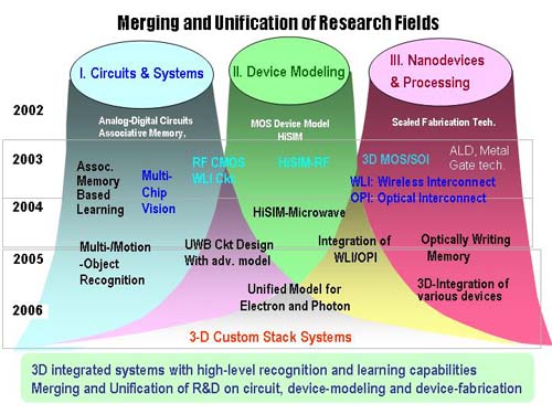
HiSIM device modeling is situated between these three-research areas. At present, we are integrating these three research pillars to create new academic and technical fields of study. The HiSIM model has been extended and is now applicable to the microwave frequency domain. Ongoing research at the COE will result in further extensions to photon and electron fusion device models. Our research fields will be united with this HiSIM device model as a major focal point.
Currently, we are engaged in research into high-frequency circuit design technologies utilizing HiSIM model for wireless interconnections with low power dissipation. We are also studying the architecture of the vision system and algorithms for moving object recognition to establish a system with advanced recognition/learning capabilities.
In device processing, we will develop three-dimensional MOS devices, integrated antennas, integrated optical components, and optical sensor/memory devices using a quantum dot structure.
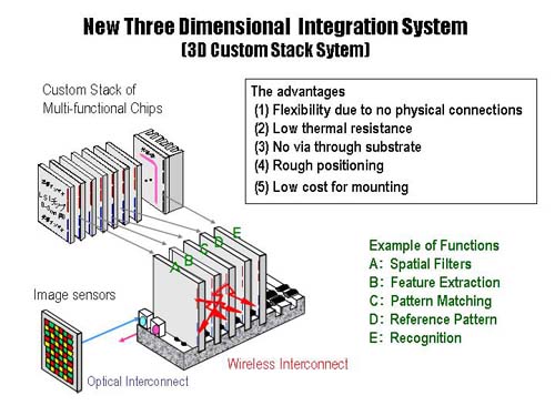
To demonstrate the capability of our technology, a three-dimensional custom stack system will be built.
Currently, we are engaged in attempts to realize a three-dimensional integration system capable of interconnection between stacked multiple chips using wireless communication. As an example of such a system, Fig. 3 shows the planned image recognition system consisting of multiple chips with various functions, including a spatial filter, feature extraction, and matching.
New academic areas of interest include electromagnetic wave transmission theory in semiconductors, integration design techniques of integration antennas and circuits, and techniques for the integration of Ultra Wide Band communication technology.
We produce many high-quality doctorate-level researchers
By extending graduate school education linked directly to advanced research, we will produce highly capable doctorate-level researchers who will make great contributions as future leaders in the fields of science and technology. The Semiconductor Electronics and Integration Science department will be established in the Graduate School of Advanced Science at Hiroshima University. Our aim is to provide high quality education linked directly to advanced research.
Utilizing high level facilities such as the super clean room, device fabrication equipments, and LSI tester, we will foster the development of talented individuals with proven ability to perform valuable research in a wide range of fields, from devices to systems. A training program will be established to provide opportunities for high-level doctorate students to master not only advanced technology but also to develop a global point of view. Moreover, we are currently designing a new educational training program to further the development of logical thinking and planning abilities.
|