|
Profile |
|
|

| Name and Affiliation |

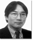
Kentaro Shibahara
shiba sxsys.hiroshima-u.ac.jp sxsys.hiroshima-u.ac.jp
Associate Professor
Research Center for Nano-devices and Systems
Hiroshima University |
| Education and Professional Background |
| 1983, 1985 and 1988 |
B.E., M.E., and D.E. degrees from Kyoto University
|
| 1988-1993 |
Microelectronics Research Laboratories, NEC Corporation |
| 1993-1995 |
ULSI Device Development Labratories, NEC Corporation |
| 1995-1996 |
Associate Professor of Research Center for Integrated Systems, Hiroshima University |
| 1996- |
Associate Professor of Research Center for Nanodevices and Systems, Hiroshima University |
|
| Academic Societies |
JSAP, IEICE, IEEE, MRS |
| World Class Research Results |
Ulta-shallow low resistive junction formation and its application to nano-scale MOSFETs
Metal gate workfunction tuning technologies |
| Pioneering Research Results |
Analysis of Vth fluctuation in ultra-thin oxide gate MOSFETs
10 nm junction formation utlizing KrF excimer laser annealing |
| Industrial and Nation-wide Cooperation |
STARC (2001-)
Komatsu (2001-2002)
NEC Hiroshima (2002-2003)
MIRAI Pj (2002-)
Selete (2004-) |
| Important Publications |
| 1. |
K. Shibahara,
“Ultra-Shallow Jucntion Formation with Antimony
Implantation” (Invited Paper), IEICE Trans. Electron.,
Vol. E85-C, 97 (2002), pp. 1091-10,. |
| 2. |
D. Notsu, N. Ikechi,
Y. Aoki, N. Kawakami and K. Shibahara , “Fabrication
of 100 nm width Fine Active-Region Using LOCOS
Isolation”, IEICE Trans. Electron., Vol. E85-C,
(2002), pp. 1119-1123. |
| 3. |
T. Amada, N. Maeda,
and K. Shibahara , “Degradation in a Molybdenum-Gate
MOS Structure Caused by N+ Ion Implantation for
Work Function Control”, Mat. Res. Soc. Symp.
Proc., vol. 716, (2002), pp.B7.5.1-B7.5.6. |
| 4. |
M. Koh, W. Mizubayashi,
K. Iwamoto, H. Murakami, T. Ono, M. Tsuno, T.
Mihara, K. Shibahara, S. Miyazaki and M. Hirose,
“Limit of Gate Oxide Thickness Scaling in MOSFETs
due to Apparent Threshold Voltage Fluctuation
Induced by Tunnel Leakage Current”, IEEE Trans.
Electron Devices, Vol. 48 No. 2, (2001), pp.
259-264. |
| 5. |
K. Shibahara, K. Egusa
and K. Kamesaki and H. Furumoto, “Improvement
in Antimony-Doped Ultra Shallow Junction Sheet
Resistance by Dopant Pileup Reduction at the
SiO2/Si Interface”, Jpn. J.
Appl. Phys. Vol. 39, (2000), pp. 2194-2197. |
|
| Laboratory Page |
http://www.rcns.hiroshima-u.ac.jp/ |
| Personal Page |
http://www.rcns.hiroshima-u.ac.jp/shiba/ |
|
|
|
|
|
|


