|
Profile |
|
|

| Name and Affiliation |

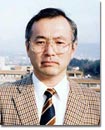
Takamaro Kikkawa
kikkawa sxsys.hiroshima-u.ac.jp sxsys.hiroshima-u.ac.jp
Professor:
Research Center for Nanodevices and Systems, Hiroshima University, Japan
Graduate School of Advanced Science of Matter, Hiroshima University, Japan
Senior Research Scientist:
National Institute of Advanced Industrial Science and Technology, Japan
|
| Education and Professional Background |
| [Education] |
| 1974 |
B.S., Electronic Engineering, Shizuoka University, Japan |
| 1976 |
M.S., Electronic Engineering, Shizuoka University, Japan |
| 1994 |
Ph.D., Electronic System, Tokyo Institute of Technology, Japan |
| [Professional History] |
| 1974 |
Engineer, NEC Corporation, Japan |
| 1983 |
Visiting Scientist, Massachusetts Institute of Technology, USA |
| 1988 |
Research Manager, Microelectronics Research Laboratory, NEC Corporation |
| 1994 |
Senior Manager, USLI Device Development Laboratory, NEC Corporation |
| 1998 present |
Professor, Hiroshima University, Japan |
| 2001 present |
Senior Research Scientist, National Institute of Advanced Industrial Science and Technology |
| 2001 present |
Group Leader, Low-k/Interconnect Technology Group, Japan’s National Project MIRAI |
|
| Academic Societies |
Japan Society of Applied Physics, Member,
2003-present Councilor
1999-2002 Board of Directors
2001 SSDM Program co-chair
1998-2001 SSDM Subcommittee chair
The Institute of Electrical and Electronics Engineers Inc. (IEEE), Senior Member
2000-present IITC Executive committee member Å@
1998–1999 IITC General Co-chair
1995-1996 IEDM Subcommittee member
The Materials Research Society (MRS), Member
2002 Symposium organizer
1998 Symposium organizer
1996 Symposium organizer
The Electrochemical Society (ECS), Active Member
Advanced Metallization Conference 2002 Asia Session, Program Chair
|
| Award |
2000 Best Paper Award of Japan Society of Applied Physics |
| World Class Research Results |
High-temperature-sputtered CoSi2 salicide process for 0.15 mm CMOS (IEDM1996)
High-temperature-sputtered TiSi2 salicide process for 0.25mm CMOS (VLSI Symp1995)
|
| Pioneering Research Results |
Photosensitive low-k dielectrics for 50 nm technology ( IEDM2000)
Ti-PECVD and TiN-LPCVD for 256MDRAM (IEDM1994,1995, 1996)
Al-Ge-Cu damascene process ( IEDM 1992, 1993, 1994)
Al-alloy interconnect for 0.25mm technology (IEDM1991
|
| Industrial and Nation-wide Cooperation |
2001-present Group Leader, Low-k/Interconnect Technology Group, Japan’s National Project MIRAI |
| Important Publications Journal Paper |
| 1. |
A.B.M. H. Rashid, S. Watanabe and T. Kikkawa, "Characteristics of Integrated Antenna on Si for On-Chip Wireless Interconnect", Japanese Journal of Applied Physics, Vol. 42, No. 4B, April 2003, pp. 2204-2209. |
| 2.Å@ |
K. Yamada, Y. Oku, N. Hata, S. Takada and T. Kikkawa, "Effects of surfactants on the properties of ordered periodic porous silica films," Japanese Journal of Applied Phys, Vol.42, No. 4B, April 2003, pp.1840-1842. |
| 3. |
S. Kuroki, T. Kikkawa, H. Kochiya, and S. Shishiguchi, "Direct Patterning of Low-k Dielectric Films using X-Ray Lithography," Jpn. J. Appl. Phys. , vol.42, No.4B, (2003) pp.1907-1910. |
| 4. |
A.B.M. H. Rashid, S. Watanabe and T. Kikkawa, "High Transmission Gain Integrated Antenna on Extremely High Resistivity Si for ULSI Wireless Interconnect", IEEE Electron Device Letters, Vol. 23, No.12, December 2002, pp.731-733. |
| 5. |
T. Kikkawa, N. Fujiwara, H. Yamada, S. Miyazaki, M. Hirose and F. N.ishiyama, "Energy Band Structure of Ru/(Ba,Sr)TiO3 /Si Capacitor Deposited by Inductively-Coupled Plasma-Assisted Radio-Å@Frequency-Magnetron Plasma Sputtering," Appl. Phys. Lett. vol.81, no.15, (2002) pp.2821-2823. |
| 6. |
T. Kikkawa, T. Nagahara, and H. Matsuo, "Direct patterning of photosensitive low-dielectric-constant films using electron beam lithography", Appl. Phys. Lett. Vol. 78, No. 17 (2001) pp.2567-2569. |
| 7. |
S. Mukaigawa, T. Aoki, Y. Shimizu, and T. Kikkawa, "MeasurementÅ@of Copper Drift in Methylsilsesquiazane-Methylsilsesquioxane DielectricÅ@Films", Jpn. J. Appl. Phys. Part I, No.4B, Vol. 39 (2000) pp.2189-2193. |
| 8. |
T. Kikkawa, Multilevel interconnect technologies for scaling”, Trans. Institute of electronics, information, and communication engineers, Japan, vol.J83-C, No.2, 2000, pp.105-117. |
| 9. |
T. Kikkawa, T. Nagahara, and H. Matsuo, "Direct patterning of photosensitive low-dielectric-constant films using electron beam lithography", Appl. Phys. Lett. Vol. 78, No. 17 (2001) pp.2567-2569. |
| 10. |
T. Kikkawa, ULSI scaling and multilevel interconnect technologies”, Oyobutsuri (in Japanese), Japan Society of Applied Physics, vol.68, No.11, 1999, pp.1215-1225. |
| 11. |
K. Inoue, K. Mikagi, S. Chikaki, and T. Kikkawa, "A New Cobalt Salicide Technology for 0.15 um CMOS Devices", IEEE Trans on Electron. Devices, vol.45, No.11, pp. 2312-2318, 1998 |
| 12. |
K. Ueno, T. Kikkawa, and V. Donnely, "Cleaning of CHF3 Plasma-Etched SiO2/SiN/Cu Via Structures with Dilute Hydrofluoric Acid Solutions", Journal of Electrochem. Soc. 144(7), pp. 2565-2572, 1997 |
| 13. |
T. Taguwa, K. Urabe, Y. Yamada, T. Kikkawa and M. Sekine, "Low contact resistance metallization for gigabit scale DRAM using fully dry cleaning by Ar/H2 ECR plasma", IEEE Trans. on Electron Devices ED-44, pp. 588-594, 1997. |
| 14. |
R.T.Tung, FK. Fujii, K. Kikuta, C.Chikaki, and T. Kikkawa, “Growth of TiSi2 from codeposited TiSix layers and interface layers”, Appl. Phys. Lett. 70 (18), 1997, pp.2386-2388. |
| 15. |
K. Kikuta Y. Hayashi, T. Nakajima, K. Harashima and T. Kikkawa, "Al-Ge-Cu multilevel damascene process using low-temperature reflow sputtering and chemical mechanical polishing", IEEE Trans. Electron Devices, vol.43, no.5, pp.739-745, 1996 |
| 16. |
K. Kikuta and T. Kikkawa, "Electromigration characteristics for Al-Ge-Cu", J. Electrochem. Soc. vol.143, no.3, pp.1088-1092, 1996. |
| 17. |
Y. Teraoka, H. Aoki, E. Ikawa, T. Kikkawa, I. Nishiyama, "Observation of sidewall contamination in submicron holes by thermal desorption spectroscopy ", Journal of Vac. Sci. Technol. A, vol.13, no.6, pp.2197-2200, 1995. |
| 18. |
Y. Teraoka, I. Nishiyama, H. Aoki, E. Ikawa, T. Kikkawa, "Thermal desorption spectroscopic analysis for residual chlorine on Al-Si-Cu afterÅ@ECR plasma etching ", Journal of Vac. Sci. Technol. A, vol.13, no.6, pp.2935-2938, 1995
|
| 19. |
K. Ueno, T. Kikkawa, K. Tokashiki, "Reactive ion etching of silicon oxynitride formed by plasma-enhanced chemical vapor deposition", Journal of Vac. Sci. Technol. B, vol.13, no.4, pp.1447-1450, 1995.
|
|
| Laboratory Page |
http://www.rcns.hiroshima-u.ac.jp/ |
| Personal Page |
http://www.rcns.hiroshima-u.ac.jp/kikkawa/ |
|
|
|
|
|
|


